| CPC H01L 23/481 (2013.01) [H01L 21/76877 (2013.01); H01L 21/76898 (2013.01); H01L 24/08 (2013.01); H01L 24/32 (2013.01); H01L 24/83 (2013.01); H01L 25/0657 (2013.01); H01L 2224/08146 (2013.01); H01L 2224/32145 (2013.01); H01L 2224/8319 (2013.01); H01L 2225/06541 (2013.01)] | 8 Claims |

|
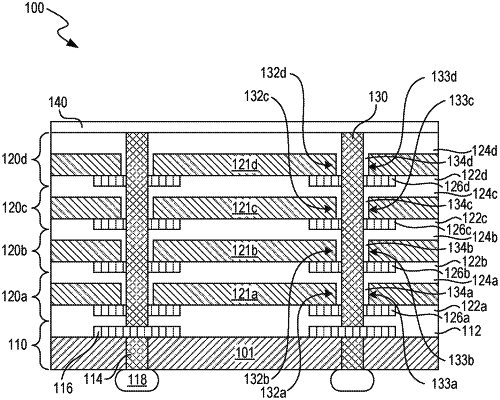
1. A semiconductor device assembly, comprising:
a base die, including:
a semiconductor substrate including an upper surface,
a base conductive pad at the upper surface, and
a base dielectric layer disposed over the base conductive pad and the upper surface;
a plurality of dies, each including:
a semiconductor substrate including an upper surface and a lower surface,
a conductive pad at the lower surface having a bottom surface opposite the lower surface,
a lower dielectric layer disposed over the conductive pad and the lower surface,
an opening extending through the semiconductor substrate and the conductive pad from the bottom surface to the upper surface, and defining an opening side wall of the semiconductor substrate and a side surface of the conductive pad,
a non-conductive liner coating the opening side wall, and
an upper dielectric layer disposed over the upper surface, wherein the plurality of dies is stacked over the base die such that the opening of each of the plurality of dies is vertically aligned with the base conductive pad; and
a monolithic conductive column extending from the base conductive pad through the opening of each of the plurality of dies and in direct contact with the side surface of the conductive pad of each of the plurality of dies.
|