| CPC H01L 23/3677 (2013.01) [H01L 21/4882 (2013.01); H01L 23/31 (2013.01); H01L 23/373 (2013.01)] | 20 Claims |

|
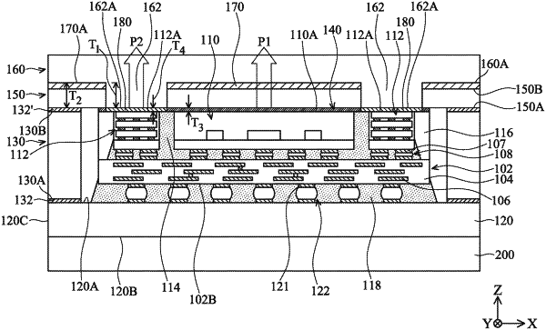
1. A semiconductor die package, comprising:
a package substrate having a first surface;
a semiconductor device disposed over the first surface of the package substrate;
a ring structure attached to the first surface of the package substrate and surrounding the semiconductor device;
a lid structure attached to the ring structure and disposed over the semiconductor device, wherein the lid structure has a first opening exposing a first part of the semiconductor device;
a heat sink disposed over the lid structure and having a first portion and a second portion, wherein the first portion is attached to an upper surface of the lid structure, and the second portion extends into the first opening of the lid structure and is attached to an upper surface of the first part of the semiconductor device;
a first thermal interface material (TIM) layer interposed between a bottom surface of the lid structure and an upper surface of a second part of the semiconductor device; and
a second TIM layer interposed between a bottom surface of the second portion of the heat sink and the upper surface of the first part of the semiconductor device, wherein the first TIM layer has a thermal conductivity higher than a thermal conductivity of the second TIM layer.
|