| CPC H01L 23/3121 (2013.01) [H01L 21/4857 (2013.01); H01L 21/568 (2013.01); H01L 23/31 (2013.01); H01L 23/3157 (2013.01); H01L 23/49816 (2013.01); H01L 23/4985 (2013.01); H01L 23/5385 (2013.01); H01L 23/5386 (2013.01); H01L 23/5387 (2013.01); H01L 24/24 (2013.01); H01L 25/0655 (2013.01); H01L 25/105 (2013.01); H05K 1/0278 (2013.01); H01L 23/481 (2013.01); H01L 23/5384 (2013.01); H01L 2224/24137 (2013.01); H01L 2225/06548 (2013.01); H01L 2924/18162 (2013.01)] | 12 Claims |

|
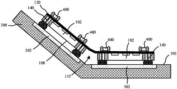
1. An electronic device comprising:
a first landing area and a second landing area; and
a flexible package mounted on the first landing area and the second landing area, the flexible package comprising:
a first die with a first face and a first back side opposite the first face, the first face including first landing pads;
a second die with a second face and a second back side opposite the second face, the second face including second landing pads;
wherein the first die and the second die encapsulated in a molding compound layer;
a compliant redistribution layer (RDL) spanning the molding compound layer, the first die, and the second die, wherein the compliant RDL includes electrical routing formed directly on the first landing pads of the first die and directly on the second landing pads of the second die;
a notch within the molding compound layer directly laterally between the first die and the second die and defining a region of the compliant RDL directly underneath the notch;
wherein the compliant RDL is twisted or bent out of plane in the region underneath the notch such that the first face and the second face are out of plane with one another;
a first vertical interconnect extending through the molding compound layer, and a second vertical interconnect extending through the molding compound layer, the first vertical interconnect including a first back side and the second vertical interconnect including a second back side;
wherein the notch separates the molding compound layer into a first molding compound region that encapsulates the first die and the first vertical interconnect and a second molding compound region that encapsulates the second die and the second vertical interconnect;
wherein the first back side of the first die, the first back side of the first vertical interconnect and a first back side of the first molding compound region form a first planarized surface;
wherein the second back side of the second die, the second back side of the second vertical interconnect and a second back side of the second molding compound region form a second planarized surface; and
wherein the first vertical interconnect is bonded to the first landing area with a first conductive bump, and the second vertical interconnect is bonded to the second landing area with a second conductive bump.
|