| CPC H01L 22/12 (2013.01) [G01B 3/004 (2013.01); H01L 21/67253 (2013.01)] | 16 Claims |
|
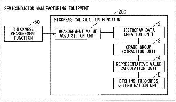
1. Semiconductor manufacturing equipment configured to perform processing for manufacturing a semiconductor on a wafer, the semiconductor manufacturing equipment comprising
a thickness calculation function,
the thickness calculation function including
a measurement value acquisition unit configured to acquire a plurality of measurement values at different measurement positions of the wafer from a thickness measurement function configured to measure a thickness of the wafer or a thickness measurement object deposited on the wafer along a surface of the wafer,
a histogram data creation unit configured to create histogram data based on the plurality of measurement values, and
a grade group extraction unit configured to extract a grade group from the histogram data,
the grade group including sequential grades having frequencies equal to or greater than a predetermined frequency,
the thickness calculation function further including a representative value calculation unit configured to calculate a representative value of a thickness of a measurement region based on the grades included in the extracted grade group.
|