| CPC H01L 21/78 (2013.01) [H01L 21/56 (2013.01); H01L 21/561 (2013.01); H01L 21/568 (2013.01); H01L 21/6835 (2013.01); H01L 23/3128 (2013.01); H01L 23/3135 (2013.01); H01L 23/544 (2013.01); H01L 23/585 (2013.01); H01L 24/05 (2013.01); H01L 24/15 (2013.01); H01L 24/19 (2013.01); H01L 24/20 (2013.01); H01L 24/14 (2013.01); H01L 24/17 (2013.01); H01L 2221/68345 (2013.01); H01L 2221/68359 (2013.01); H01L 2221/68372 (2013.01); H01L 2223/5442 (2013.01); H01L 2223/54426 (2013.01); H01L 2223/5448 (2013.01); H01L 2224/02331 (2013.01); H01L 2224/0401 (2013.01); H01L 2224/04105 (2013.01); H01L 2224/0603 (2013.01); H01L 2224/12105 (2013.01); H01L 2224/13023 (2013.01); H01L 2224/13024 (2013.01); H01L 2224/13025 (2013.01); H01L 2224/1403 (2013.01); H01L 2224/16265 (2013.01); H01L 2224/1703 (2013.01); H01L 2224/214 (2013.01); H01L 2224/81005 (2013.01); H01L 2224/94 (2013.01)] | 20 Claims |

|
1. A package structure, comprising:
an integrated circuit component, comprising:
a semiconductor die;
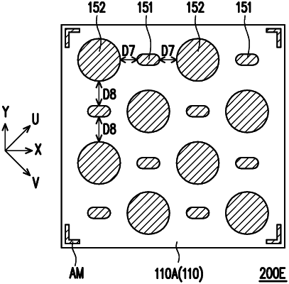
conductive vias, disposed on and electrically coupled to the semiconductor die, wherein each conductive via of a first group of the conductive vias has a first maximum size, each conductive via of a second group of the conductive vias has a second maximum size, and the first maximum size is less than the second maximum size in a vertical projection on the semiconductor die;
alignment marks, disposed on and electrically isolated from the semiconductor die, wherein a thickness of each of the alignment marks is less than a thickness of each of the conductive vias along a stacking direction of the conductive vias and the semiconductor die; and
a protection layer, covering the semiconductor die and at least in contact with sidewalls of the conductive vias and sidewalls of the alignment marks, wherein top surfaces of the alignment marks, top surfaces of the first group of the conductive vias and top surfaces of the second group of the conductive vias are substantially coplanar to a top surface of the protection layer; and
a first redistribution circuit structure, disposed on and electrically connected to the integrated circuit component, wherein the first redistribution circuit structure is electrically connected to the conductive vias and is electrically isolated from the alignment marks.
|