| CPC H01L 21/78 (2013.01) [H01L 33/0095 (2013.01); H01S 5/0202 (2013.01); H01S 5/04256 (2019.08)] | 10 Claims |

|
1. A semiconductor device production method, comprising:
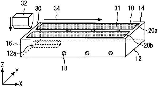
providing a first electrode and a second electrode on a rear surface of a substrate, a plurality of active regions being formed on the substrate, the active regions being closer to a front surface of the substrate than to the rear surface of the substrate, the front surface of the substrate being opposite to the rear surface of the substrate, and providing at least one laminated object less brittle than the substrate at part of a flat region between the first electrode and the second electrode so as to position the at least one laminated object directly below the active regions; and
cleaving the substrate together with the at least one laminated object in a state of having the at least one laminated object positioned directly above the active regions respectively, wherein
the at least one laminated object are away from the first electrode and the second electrode,
the at least one laminated object break due to the cleaving, and
during cleaving, fewer substrate scraps are generated directly below the at least one laminated object compared with portions of the substrate that are not directly below the at least one laminated object.
|