| CPC H01L 21/76807 (2013.01) [H01L 21/76829 (2013.01); H01L 21/76877 (2013.01); H01L 23/5226 (2013.01); H01L 21/31116 (2013.01); H01L 21/31144 (2013.01); H01L 21/32136 (2013.01); H01L 21/32139 (2013.01); H01L 2221/1031 (2013.01)] | 20 Claims |
|
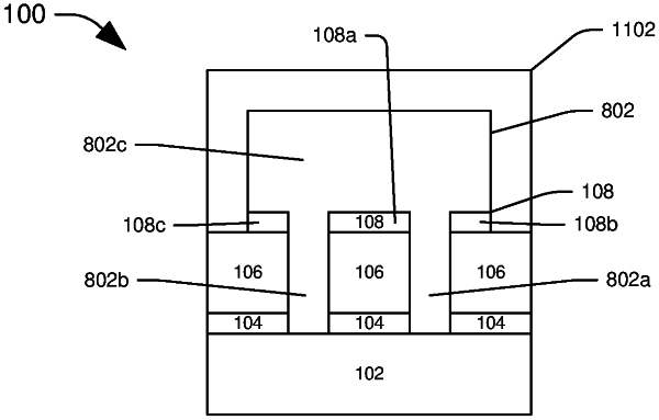
10. A semiconductor arrangement, comprising:
a metal layer overlying a substrate;
a conductive structure penetrating through the metal layer to the substrate and contacting the metal layer; and
a first dielectric layer surrounding at least four sides of the conductive structure and contacting the metal layer.
|