| CPC H01L 21/76254 (2013.01) [H01L 21/84 (2013.01); H01L 27/1207 (2013.01); H01L 21/02532 (2013.01)] | 16 Claims |

|
1. A substrate, comprising:
a receiver substrate;
an active layer comprising single-crystal semiconductor material; and
an electrically insulating silicon oxide layer interposed between the active layer and the receiver substrate; and
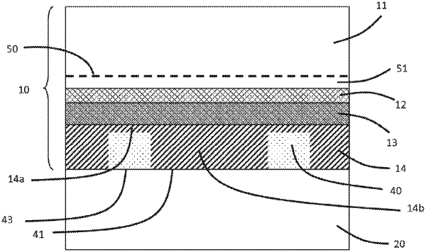
a polycrystalline silicon layer on the receiver substrate, the polycrystalline silicon layer coated with the electrically insulating silicon oxide layer so as to define a first portion of the electrically insulating silicon oxide layer having a first thickness and interposed between the polycrystalline silicon layer and the active layer, and a second portion of the electrically insulating silicon oxide layer having a second thickness greater than the first thickness, the second portion being located between the receiver substrate and the active layer.
|