| CPC H01L 21/3086 (2013.01) [H01L 21/823431 (2013.01); H01L 21/823468 (2013.01); H01L 29/6681 (2013.01)] | 14 Claims |

|
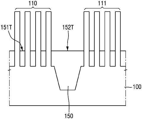
1. A method of fabricating a semiconductor device, comprising:
forming a lower mask layer, an upper mask layer, a first sacrificial layer and a second sacrificial layer, which are sequentially stacked, on a substrate;
forming a first photosensitive film pattern on the second sacrificial layer;
forming a first mandrel by etching the second sacrificial layer using the first photosensitive film pattern;
forming first spacers on sidewalls of the first mandrel;
forming a second mandrel by etching the first sacrificial layer using the first spacers;
forming second spacers on sidewalls of the second mandrel;
forming a first upper mask fin pattern and a second upper mask fin pattern, which are spaced apart from each other, by etching the upper mask layer using the second spacers;
forming a third sacrificial layer on the first upper mask fin pattern and the second upper mask fin pattern and on the lower mask layer;
forming a second photosensitive film pattern on the third sacrificial layer between the first upper mask fin pattern and the second upper mask fin pattern;
forming lower mask fin patterns on the substrate by etching the lower mask layer using the second photosensitive film pattern, the first upper mask fin pattern, and the second upper mask fin pattern; and
forming fin patterns by etching the substrate using the lower mask fin patterns,
wherein the forming of the lower mask fin patterns comprises:
forming a lower dummy mask pattern by etching the third sacrificial layer and the lower mask layer using the second photosensitive film pattern;
forming a first lower mask fin pattern by etching the lower mask layer using the first upper mask fin pattern; and
forming a second lower mask fin pattern by etching the lower mask layer using the second upper mask fin pattern,
wherein the forming fin patterns comprises:
forming a dummy fin pattern by etching at least a first portion of the substrate using the lower dummy mask pattern,
forming a first fin pattern by etching at least a second portion of the substrate using the first lower mask fin patterns, and
forming a second fin pattern by etching at least a third portion of the substrate using the second lower mask fin patterns.
|