| CPC H01L 21/0228 (2013.01) [C23C 16/045 (2013.01); H01L 21/02274 (2013.01); H01L 21/02296 (2013.01); H01L 21/0262 (2013.01); H01L 21/28556 (2013.01); H01L 21/76843 (2013.01); H01L 28/91 (2013.01)] | 20 Claims |

|
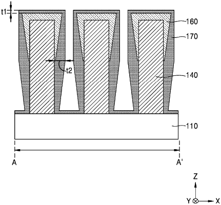
1. A semiconductor device comprising:
a substrate;
a first conductive pattern on the substrate, the first conductive pattern having an upper portion and a lower portion, the lower portion extending from the substrate to a first distance along the first conductive pattern, and the upper portion extending from the first distance;
a second conductive pattern on the upper portion of the first conductive pattern, the second conductive pattern not being on the lower portion of the first conductive pattern; and
a third conductive pattern on the first conductive pattern and the second conductive pattern,
wherein
the third conductive pattern includes a first portion on the lower portion of the first conductive pattern, a second portion on the second conductive pattern, and a third portion adjacent to a boundary between the upper portion of the first conductive pattern and the lower portion of the first conductive pattern,
the third portion of the third conductive pattern is between the first portion of the third conductive pattern and the second portion of the third conductive pattern, and
a thickness of the third portion of the third conductive pattern is greater than a thickness of at least one of the first portion of the third conductive pattern or the second portion of the third conductive pattern.
|