| CPC H01L 21/02274 (2013.01) [C23C 16/042 (2013.01); C23C 16/345 (2013.01); C23C 16/401 (2013.01); C23C 16/45536 (2013.01); C23C 16/52 (2013.01); H01J 37/32082 (2013.01); H01J 37/32449 (2013.01); H01L 21/0228 (2013.01); H01L 21/0337 (2013.01); H01J 2237/332 (2013.01); H01L 21/02142 (2013.01); H01L 21/02164 (2013.01); H01L 21/0217 (2013.01); H01L 21/02172 (2013.01)] | 25 Claims |

|
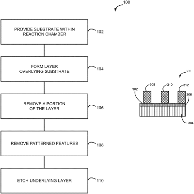
1. A method of forming patterned structures using a multiple patterning process, the method comprising the steps of:
providing a substrate within a reaction chamber, the substrate comprising a surface comprising patterned features; and
forming a layer overlying the substrate, wherein the step of forming the layer comprises:
providing a precursor to the reaction chamber for a precursor pulse period;
providing a reactant to the reaction chamber for a reactant pulse period;
applying a first plasma power having a first frequency less than 1 MHz for a first plasma power period; and
optionally applying a second plasma power having a second frequency for a second plasma power period,
wherein the first frequency of the first plasma power is less than 1 MHz and the second frequency of the second plasma power is higher compared to the first frequency of the first plasma power.
|