| CPC H01J 49/025 (2013.01) | 8 Claims |
|
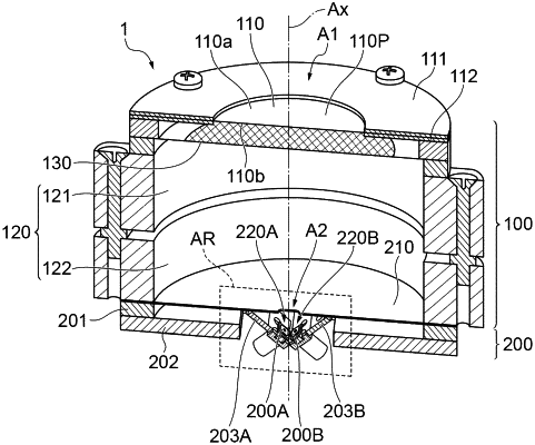
1. An ion detector comprising:
a microchannel plate configured to generate secondary electrons upon reception of ions incident thereon and multiply and output the generated secondary electrons;
a plurality of electron impact-type diodes having effective regions narrower than an effective region of the microchannel plate, configured to receive the secondary electrons incident thereon output from the microchannel plate, and multiply and detect the secondary electrons;
a focus electrode disposed between the microchannel plate and the electron impact-type diodes and configured to focus the secondary electrons toward the electron impact-type diodes; and
a voltage supply part configured to apply a drive voltage to each of the plurality of electron impact-type diodes,
wherein the voltage supply part applies drive voltages having values different from each other to at least two respective electron impact-type diodes of the plurality of electron impact-type diodes to make gains thereof different from each other,
wherein the plurality of electron impact-type diodes include the effective region of the electron impact-type diode and a non-effective region positioned around the effective region of the electron impact-type diode when viewed in an incident direction of secondary electrons in the electron impact-type diodes,
wherein when viewed in the incident direction, the effective region of the electron impact-type diode is unevenly distributed in at least one direction with respect to a center of the non-effective region, and
wherein at least the two electron impact-type diodes are disposed such that sides thereof having the unevenly distributed effective regions of the electron impact-type diode are adjacent to each other.
|