| CPC H01G 4/008 (2013.01) [B22F 1/05 (2022.01); C22C 19/03 (2013.01); H01G 4/30 (2013.01); B22F 2301/15 (2013.01); B22F 2304/05 (2013.01)] | 14 Claims |
|
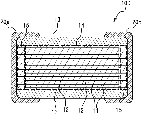
1. A ceramic electronic device comprising:
a multilayer chip in which each of a plurality of dielectric layers of which a main component is ceramic, and each of a plurality of internal electrode layers are alternately stacked,
wherein the plurality of internal electrode layers include Ni, S and Sn,
wherein each of the plurality of internal electrode layers includes a Ni layer of which a main component is Ni, in a center portion thereof in a thickness direction,
wherein each of the plurality of internal electrode layers includes a high Sn concentration portion and a high S concentration portion,
wherein the high Sn concentration portion has a higher Sn concentration than the Ni layer and is closer to each of the plurality of dielectric layers than the Ni layer, and
wherein the high S concentration portion has a higher S concentration than the high Sn concentration portion and is closer to each of the plurality of dielectric layers than the high Sn concentration portion.
|