| CPC G11C 8/16 (2013.01) [G06F 30/392 (2020.01); G11C 11/418 (2013.01); G11C 11/419 (2013.01)] | 15 Claims |

|
1. A circuit comprising:
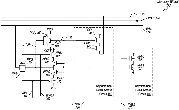
an array of memory bit cells for storing data, wherein a given memory bit cell of the array comprises:
a data storage circuit;
a first asymmetrical read access circuit configured to receive a complementary value of the data stored by the data storage circuit; and
a second asymmetrical read access circuit configured to receive the complementary value of the data stored by the data storage circuit, wherein the second asymmetrical read access circuit comprises more transistors of an n-type or a p-type than the first asymmetrical read access circuit; and
wherein in response to receiving an indication of a first read operation, the first asymmetrical read access circuit is configured to:
access the complementary value of the data stored by the data storage circuit; and
convey data stored by the data storage circuit to a first read bit line.
|