| CPC G11C 7/222 (2013.01) [G06F 1/04 (2013.01); G06F 3/0604 (2013.01); G06F 3/0659 (2013.01); G06F 3/0673 (2013.01); G11C 29/023 (2013.01); G11C 29/028 (2013.01); G11C 5/145 (2013.01)] | 19 Claims |

|
1. A storage device comprising:
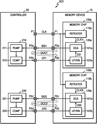
a duty sensing chip configured to generate a clock signal, the duty sensing chip comprising a plurality of duty sensing circuits, each duty sensing circuit of the plurality of duty sensing circuits respectively configured to generate a positive signal and a negative signal based on a data signal of a plurality of data signals, the data signal having a duty cycle, the positive signal and the negative signal having the duty cycle of the data signal, the negative signal having a reverse phase to a phase of the positive signal, and to generate a comparison signal based on a comparison of the positive signal and the negative signal; and
a memory device including a plurality of memory chips respectively corresponding to the plurality of duty sensing circuits, each memory chip of the plurality of memory chips respectively configured to generate a data signal of the plurality of data signals, to generate an internal clock signal based on the clock signal, the internal clock signal having a duty cycle, and to correct the duty cycle of the internal clock signal based on the comparison signal.
|