| CPC G11C 7/109 (2013.01) [G11C 7/1084 (2013.01); G11C 7/1096 (2013.01); G11C 7/22 (2013.01)] | 21 Claims |

|
1. A memory device, comprising:
a memory bank including a plurality of memory cells; and
a memory interface circuit configured to store data in the plurality of memory cells based on a command/address signal and a data signal, wherein
the memory interface circuit comprises:
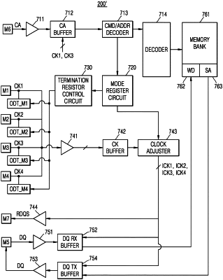
first, second, third and fourth pads configured to receive first, second, third and fourth clock signals, respectively, wherein the first and third clock signals have opposite phases from each other, the second and fourth clock signals have opposite phases from each other, and the first and second clock signals are synchronized;
a first buffer circuit configured to sample the command/address signal in response to an activation time of the first and third clock signals; and
a second buffer circuit configured to sample the data signal in response to the activation time of the first clock signal, an activation time of the second clock signal, the activation time of the third clock signal and an activation time of the fourth clock signal.
|