| CPC G11C 7/1012 (2013.01) [G06F 3/0619 (2013.01); G11C 11/4093 (2013.01); G11C 11/4096 (2013.01); G06F 3/0659 (2013.01); G06F 3/0679 (2013.01); G06F 11/1068 (2013.01); G11C 11/4082 (2013.01); G11C 2207/005 (2013.01)] | 17 Claims |

|
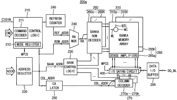
1. A semiconductor memory device comprising:
a memory cell array including a plurality of sub array blocks arranged in a first direction and in a second direction crossing the first direction, each of the plurality of sub array blocks including a plurality of memory cells;
a data input/output (I/O) buffer configured to exchange data with a memory controller through a plurality of I/O pads;
an I/O gating circuit, connected to the data I/O buffer through a plurality of data buses and connected to the memory cell array through a plurality of data I/O lines, the I/O gating circuit configured to:
receive a mapping control signal, and
based on the mapping control signal, set a mapping relationship between the plurality of sub array blocks in which the data is stored and the plurality of I/O pads through which the data is transferred; and
a control logic circuit configured to generate the mapping control signal based on identifier information about a central processing unit (CPU) of the memory controller.
|