| CPC G11C 7/065 (2013.01) [G11C 7/1039 (2013.01); G11C 7/1057 (2013.01); G11C 7/1084 (2013.01); G11C 16/3404 (2013.01)] | 20 Claims |

|
1. A memory device comprising:
a memory cell array including a plurality of memory cell groups;
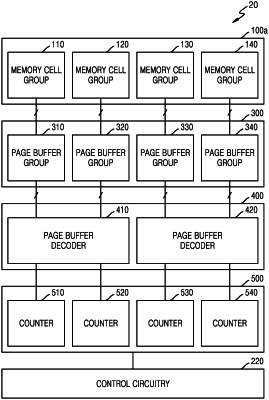
a page buffer circuit including a plurality of page buffer groups respectively connected to the plurality of memory cell groups, wherein:
each of the plurality of page buffer groups comprises a plurality of page buffer units arranged in a matrix form, and
a plurality of first page buffer units in a first stage of each page buffer group are divided into a first group configured to perform a first sensing operation according to a first sensing signal and a second group configured to perform a second sensing operation according to a second sensing signal;
a counting circuit configured to count a first number of memory cells included in a first threshold voltage region from a result of the first sensing operation, and count a second number of memory cells included in a second threshold voltage region from a result of the second sensing operation; and
a control circuit configured to determine a development time period of the plurality of first page buffer units based on a comparison result of the first number of memory cells and the second number of memory cells,
wherein the plurality of page buffer groups comprise a first page buffer group, a second page buffer group, a third page buffer group, and a fourth page buffer group, and
wherein the memory device further comprises:
a first page buffer decoder configured to generate a first current corresponding to a number of memory cells included in the first threshold voltage region from page buffer units of the first group of the first and second page buffer groups, and generate a second current corresponding to a number of memory cells included in the second threshold voltage region from page buffer units of the second group of the first and second page buffer groups; and
a second page buffer decoder configured to generate a third current corresponding to a number of memory cells included in the first threshold voltage region from page buffer units of the first group of the third and fourth page buffer groups, and generate a fourth current corresponding to a number of memory cells included in the second threshold voltage region from page buffer units of the second group of the third and fourth page buffer groups.
|