| CPC G11C 29/42 (2013.01) [G11C 7/1048 (2013.01); G11C 7/1063 (2013.01); G11C 8/18 (2013.01); G11C 29/1201 (2013.01)] | 35 Claims |

|
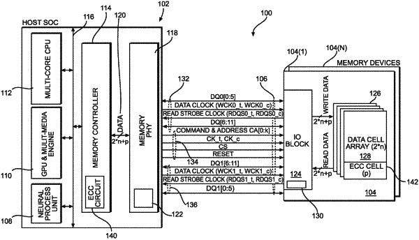
1. An integrated circuit (IC) comprising:
a memory bus interface comprising thirty-two pins, wherein:
twenty-four pins correspond to data conductors;
four pins correspond to clock conductors; and
four pins correspond to read strobe clock (RDQS) conductors; and
routing and encoding logic associated with the memory bus interface and configured to route signals to pins within the memory bus interface; and
wherein the thirty-two pins comprise a first group and a second group, wherein the first group comprises:
a first six pins of the twenty-four pins corresponding to the data conductors;
a first two pins of the four pins corresponding to the clock conductors positioned adjacent to the first six pins;
a second two pins of the four pins corresponding to the RDQS conductors adjacent to the first two pins; and
a second six pins of the twenty-four pins corresponding to the data conductors adjacent to the second two pins.
|