US 12,073,899 B2
Track charge loss based on signal and noise characteristics of memory cells collected in calibration operations
Sivagnanam Parthasarathy, Carlsbad, CA (US); James Fitzpatrick, Laguna Niguel, CA (US); Patrick Robert Khayat, San Diego, CA (US); and AbdelHakim S. Alhussien, San Jose, CA (US)
Assigned to Micron Technology, Inc., Boise, ID (US)
Filed by Micron Technology, Inc., Boise, ID (US)
Filed on Nov. 29, 2021, as Appl. No. 17/536,462.
Application 17/536,462 is a continuation of application No. 16/988,360, filed on Aug. 7, 2020, granted, now 11,227,666.
Prior Publication US 2022/0084614 A1, Mar. 17, 2022
This patent is subject to a terminal disclaimer.
Int. Cl. G11C 29/12 (2006.01); G06F 18/214 (2023.01); G06N 20/00 (2019.01); G11C 7/02 (2006.01); G11C 29/14 (2006.01); G11C 29/44 (2006.01)
CPC G11C 29/12005 (2013.01) [G06F 18/214 (2023.01); G06N 20/00 (2019.01); G11C 7/02 (2013.01); G11C 29/14 (2013.01); G11C 29/44 (2013.01)] 20 Claims
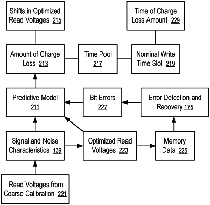
OG exemplary drawing
 
1. A device, comprising:
memory cells; and
a logic circuit configured to:
receive data representative of signal and noise characteristics of the memory cells;
determine, based on the signal and noise characteristics, a read voltage to read the memory cells; and
calculate, based at least in part on the signal and noise characteristics, an amount of charge loss in the memory cells; and
a read circuit configured to apply voltages to the memory cells to determine states of the memory cells under the voltages applied to the memory cells; and
an integrated circuit package configured to enclose the memory cells, the logic circuit, and the read circuit.