| CPC G11C 29/023 (2013.01) [G06F 12/023 (2013.01); G06F 2212/202 (2013.01)] | 34 Claims |

|
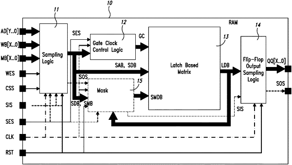
1. A random access memory (RAM), comprising:
an array of storage elements arranged in rows and columns, wherein the rows of the storage elements correspond to respective memory locations of the RAM, the storage elements of a row have a common gated-clock input and respective data inputs, and each row of the array of storage elements comprises a plurality of D type latches;
an address input, which, in operation, receives a memory address identifying a memory location in the RAM; and
clock gating circuitry having an input coupled to the address input, wherein the clock gating circuitry comprises:
test mode control logic, which, in operation, generates a test mode enable signal based on a test mode signal and a scan enable signal; and
a plurality of clock gating cells, which, in operation, generate respective gated-clock signals for the rows of the array of storage elements based on the memory address received at the address input and the test mode enable signal.
|