| CPC G11C 16/3459 (2013.01) [G11C 16/08 (2013.01); G11C 16/102 (2013.01); G11C 16/24 (2013.01); G11C 16/26 (2013.01); G11C 16/30 (2013.01)] | 20 Claims |

|
1. A memory device comprising:
a memory array; and
control logic, operatively coupled with the memory array, to perform operations comprising:
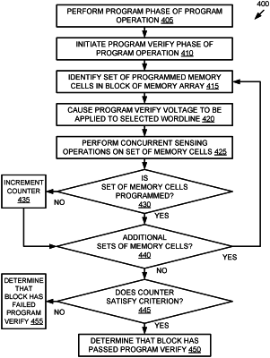
identifying a set of memory cells in a block of the memory array, wherein the set of memory cells comprises two or more memory cells programmed during a program phase of a program operation and associated with a selected wordline of the memory array;
causing a program verify voltage to be applied to the selected wordline during a program verify phase of the program operation;
performing concurrent sensing operations on the set of memory cells to determine whether each memory cell in the set of memory cells was programmed to at least the program verify voltage during the program phase of the program operation; and
responsive to determining that each memory cell in the set of memory cells was not programmed to at least the program verify voltage during the program phase of the program operation, incrementing a value of a counter, wherein the value of the counter represents whether the block of the memory array has passed the program verify phase of the program operation.
|