| CPC G11C 16/24 (2013.01) [G11C 7/1039 (2013.01); G11C 16/0433 (2013.01); G11C 16/10 (2013.01); G11C 16/26 (2013.01)] | 20 Claims |

|
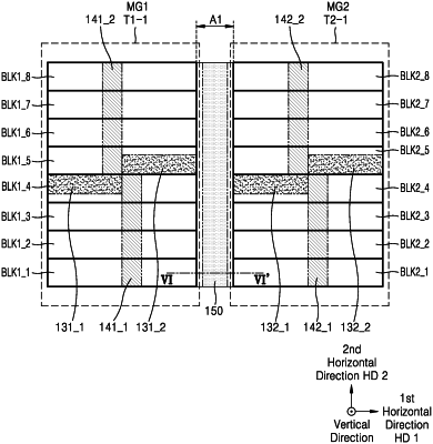
1. A method for internally transferring data in a non-volatile memory including an upper semiconductor layer vertically stacked on a lower semiconductor layer, wherein the upper semiconductor layer includes a first memory group and a second memory group separated in a first horizontal direction by a separation region, and the lower semiconductor layer includes a bypass circuit underlying at least a portion of the separation region, the method comprising:
sensing first data stored in a first memory block of the first memory group using a first page buffer associated with the first memory group and storing the first data in the bypass circuit;
transferring the first data stored in the bypass circuit to a second page buffer associated with the second memory group;
programming the first data transferred to the second page buffer in a first memory block of the second memory group;
sensing second data stored in a second memory block of the first memory group using the first page buffer and storing the second data together with the first data in the bypass circuit;
transferring the second data stored in the bypass circuit together with the first data stored in the bypass circuit to the second page buffer;
programming the first data together with the second data transferred to the second page buffer in the second memory group as a unitary block of data; and
after storing the first data and the second data in the bypass circuit, waiting until an idle time for the non-volatile memory device is detected and then transferring the first data together with the second data as a unitary block of data from the bypass circuit to the second page buffer.
|