| CPC G11C 16/16 (2013.01) [G11C 16/0483 (2013.01); G11C 16/107 (2013.01); G11C 16/3404 (2013.01); G11C 16/349 (2013.01); G11C 2216/16 (2013.01); G11C 2216/18 (2013.01)] | 20 Claims |

|
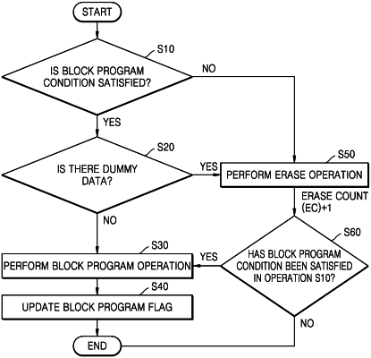
1. An operating method of a semiconductor device including a controller and a non-volatile memory device operating under control of the controller, the operating method comprising:
determining, by the controller, whether the non-volatile memory device satisfies a block program condition, wherein the block program condition is based on an erase count of a memory block and a number of deteriorated memory cells identified by performing a one-shot program operation;
based on the non-volatile memory device satisfying the block program condition, performing a block program operation a plurality of times, wherein the block program operation is associated with removing excess holes; and
based the non-volatile memory device not satisfying the block program condition, performing an erase operation, wherein the erase operation is associated with removing excess electrons.
|