| CPC G11C 16/102 (2013.01) [G11C 16/08 (2013.01); G11C 16/24 (2013.01); G11C 16/26 (2013.01)] | 24 Claims |

|
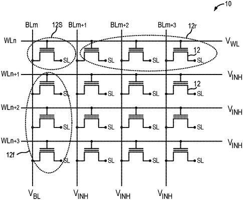
1. A method for reducing write disturb in an array of memory cells arranged in a plurality of memory pages, each memory page comprising memory cells arranged in rows and columns, the method comprising:
selecting a row of memory cells in a first memory page for a write operation to store write data into the memory cells;
determining a step order value indicative of a write step order of the write operation;
in response to the step order value having a first logical state, performing the write operation by writing data of a first logical state in all the memory cells in the selected row followed by writing data of a second logical state in at least a subset of memory cells in the selected row in response to the write data; and
in response to the step order value having a second logical state, performing the write operation by writing data of the second logical state in all the memory cells in the selected row followed by writing data of the first logical state in at least a subset of memory cells in the selected row in response to the write data.
|