| CPC G11C 16/10 (2013.01) [G06F 3/0604 (2013.01); G06F 3/064 (2013.01); G06F 3/0659 (2013.01); G06F 3/0679 (2013.01); G11C 16/0483 (2013.01); G11C 16/08 (2013.01); G11C 16/3418 (2013.01); H10B 43/27 (2023.02)] | 8 Claims |

|
1. A memory system connectable to a host device, the memory system comprising:
a nonvolatile semiconductor memory device; and
a controller configured to access the nonvolatile semiconductor memory device based on a command received from the host device, wherein
the nonvolatile semiconductor memory device includes:
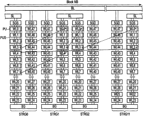
first and second strings, each of the first and second strings including a plurality of memory cells and a select transistor, the plurality of memory cells being connected in series, the select transistor being electrically connected in series with the memory cells, the memory cells including a first memory cell, a second memory cell, a third memory cell, and a fourth memory cell;
a bit line electrically connected to the first and the second strings;
a first select gate line electrically connected to a gate of the select transistor of the first string;
a second select gate line electrically connected to a gate of the select transistor of the second string;
a first word line electrically connected to gates of the first memory cell of the first string and the first memory cell of the second string;
a second word line electrically connected to gates of the second memory cell of the first string and the second memory cell of the second string;
a third word line electrically connected to gates of the third memory cell of the first string and the third memory cell of the second string; and
a fourth word line electrically connected to gates of the fourth memory cell of the first string and the fourth memory cell of the second string,
the controller is configured to perform a first write process, to perform a second write process after the first write process, to perform a third write process after the second write process, and to perform a fourth write process after the third write process, the first write process includes writing data in the first memory cell of the first string and writing data in the second memory cell of the first string after the writing in the first memory cell of the first string,
the second write process includes writing data in the first memory cell of the second string and writing data in the second memory cell of the second string after the writing in the first memory cell of the second string,
the third write process includes writing data in the third memory cell of the first string and writing data in the fourth memory cell of the first string after the writing in the third memory cell of the first string, and
the fourth write process includes writing data in the third memory cell of the second string and writing data in the fourth memory cell of the second string after the writing in the third memory cell of the second string.
|