| CPC G11C 11/419 (2013.01) [G11C 5/145 (2013.01)] | 20 Claims |

|
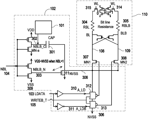
1. A write driver configured to receive a data signal, a write signal, and a negative bit line input signal and to generate a negative bit line voltage to one of two bit lines of a memory cell, the write driver comprising:
a capacitor responsive to a first node configured to provide a transition of the negative bit line voltage over a period of time; and
a voltage limiter circuit configured to control a voltage at the first node, the voltage limiter circuit being configured to limit a magnitude of the negative bit line voltage on said one of the two bit lines of the memory cell such that the magnitude does not exceed a predefined threshold.
|