| CPC G11C 11/418 (2013.01) | 20 Claims |

|
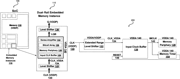
1. A level shifter circuit, comprising:
a level shifter configured to receive a first clock signal associated with a first power level (VDDP) and generate a second clock signal associated with a second power level (VDDA), wherein the second power level is greater than the first power level; and
an input clock buffer comprising a first input, wherein the first input comprises the second clock signal from the level shifter, and a second input coupled in parallel to the first input, wherein the second input comprises the first clock signal.
|