| CPC G11C 11/4091 (2013.01) [G11C 7/065 (2013.01); G11C 11/4074 (2013.01); G11C 11/4094 (2013.01); G11C 11/4096 (2013.01); G11C 11/4099 (2013.01)] | 17 Claims |

|
1. A method, comprising:
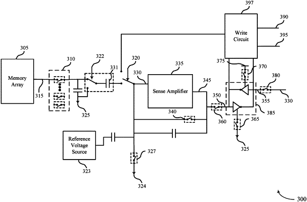
precharging an input and an output of an amplifier stage of a sense component to a first voltage based at least in part on a read operation associated with a memory cell;
activating a switch coupled with the output of the amplifier stage and a first side of a latch stage of the sense component to couple the output of the amplifier stage with the first side of the latch stage;
deactivating a second switch coupled with a second side of the latch stage and the input of the amplifier stage;
precharging at least one side of the latch stage to the first voltage based at least in part on activating the switch, deactivating the second switch, and precharging the output of the amplifier stage to the first voltage, wherein the latch stage is coupled with the amplifier stage; and
coupling a second voltage from a digit line associated with the memory cell to the input of the amplifier stage, wherein the amplifier stage generates a third voltage on the output based at least in part on coupling the second voltage to the input, and wherein the latch stage latches a logic value associated with the memory cell based at least in part on the third voltage.
|