| CPC G11C 11/4074 (2013.01) [G11C 5/06 (2013.01); G11C 11/4085 (2013.01); G11C 11/4094 (2013.01); H03K 19/01742 (2013.01)] | 20 Claims |

|
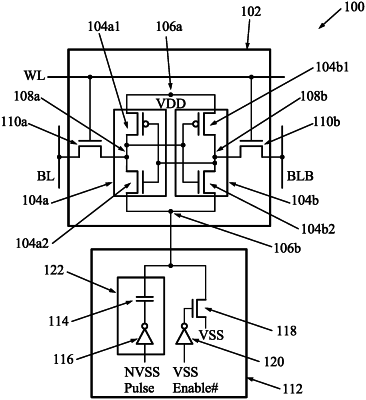
1. A memory device, comprising:
a bit cell comprising a first node and a second node;
a transistor switch connected between the second node and a ground node, wherein a gate of the transistor switch receives an enable signal; and
a negative voltage generator circuit connected to the second node in parallel to the transistor switch, wherein the negative voltage generator circuit receives an inverted enable signal pulse and is operative to pull down a voltage of the second node below a ground voltage in response to receiving the inverted enable signal pulse, and wherein the enable signal is activated before a word line activation signal, the word line activation signal indicating a read operation or a write operation in the memory device.
|