| CPC G09G 3/3266 (2013.01) [G09G 3/3233 (2013.01); G09G 3/3677 (2013.01); G09G 2310/0286 (2013.01); G09G 2310/08 (2013.01)] | 14 Claims |

|
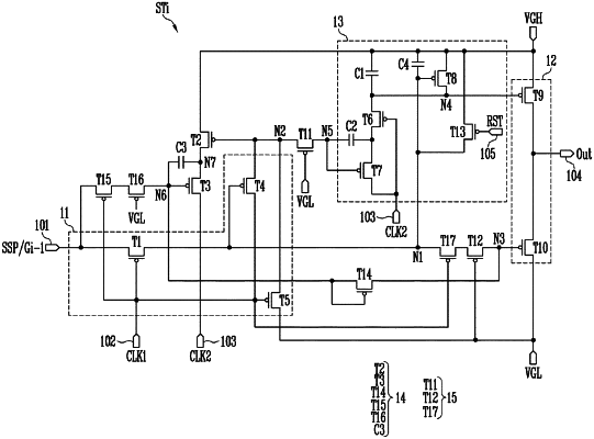
1. A scan driver comprising:
a plurality of stages,
wherein each of the plurality of stages includes:
an input portion controlling a voltage of a first node and a voltage of a second node based on signals supplied to a first input terminal and a second input terminal;
a first signal processing portion that supplies a voltage of a second power source to a fourth node based on the voltage of the first node, or electrically connects the second node and the fourth node through a fifth node based on a voltage of a first power source;
a second signal processing portion that includes a first transistor connected between a third node and a sixth node, and is connected to the first input terminal, the second input terminal, and the first power source to control a voltage of the third node based on an operation of the first transistor; and
an output portion that controls a voltage applied to the third node to be less than or equal to the voltage of the first power source, and supplies the voltage of the first power source or the voltage of the second power source to an output terminal as a scan signal based on the voltage of the third node and a voltage of the fourth node.
|