| CPC G09G 3/3258 (2013.01) [G09G 3/3291 (2013.01); G09G 2310/027 (2013.01); G09G 2320/045 (2013.01); G09G 2320/0693 (2013.01); G09G 2330/028 (2013.01)] | 12 Claims |

|
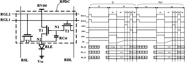
1. A pixel compensation method, comprising:
in a sensing voltage write-in stage,
providing a turning-on voltage signal to a respective first gate line to turn on a switching transistor in a respective pixel driving circuit;
providing a turning-on voltage signal to a respective second gate line to turn on a sensing transistor in the respective pixel driving circuit;
controlling a first sensing switch of a data driving integrated circuit in a conductive state to electrically connect a first reference voltage line to a respective sensing line while maintaining a second sensing switch and a third sensing switch of the data driving integrated circuit in a non-conductive state;
providing a first reference voltage signal to the respective sensing line through the first reference voltage line;
providing a sensing voltage signal to a first electrode of the switching transistor through a respective data line, the sensing voltage signal passing through the switching transistor to a first node coupled to a gate electrode of a driving transistor, a drain electrode of the switching transistor, and a first capacitor electrode of a storage capacitor;
in a data write-back stage subsequent to a charging stage and a conversion stage,
controlling the second sensing switch of the data driving integrated circuit in a conductive state to electrically connect a second reference voltage line to the respective sensing line while maintaining the first sensing switch and the third sensing switch of the data driving integrated circuit in a non-conductive state;
providing a second reference voltage signal to the respective sensing line through the second reference voltage line;
providing the turning-on voltage signal to the respective first gate line to turn on the switching transistor in a respective pixel driving circuit;
providing the turning-on voltage signal to the respective second gate line to turn on the sensing transistor in the respective pixel driving circuit; and
providing a respective data signal to the first electrode of the switching transistor through the respective data line, the respective data signal passing through the switching transistor to the first node;
wherein the second reference voltage signal has a voltage level higher than a voltage level of the first reference voltage signal.
|