| CPC G09G 3/3258 (2013.01) [G09G 3/2003 (2013.01); G09G 3/3266 (2013.01); G09G 3/3291 (2013.01); H10K 50/814 (2023.02); H10K 59/121 (2023.02); H10K 59/1213 (2023.02); H10K 59/124 (2023.02); H10K 59/131 (2023.02); H10K 59/352 (2023.02); H10K 59/353 (2023.02); H10K 59/805 (2023.02); H10K 59/82 (2023.02); G09G 2300/0426 (2013.01); G09G 2300/0443 (2013.01)] | 25 Claims |

|
1. A display substrate, comprising:
a base substrate;
a plurality of sub-pixels on the base substrate, wherein each of the plurality of sub-pixels comprises a light emitting element, the light emitting element comprises a first electrode, a light emitting layer and a second electrode which are stacked in sequence, the first electrode of the light emitting element is located at a side of the second electrode of the light emitting element away from the base substrate, the plurality of sub-pixels comprise a plurality of first color sub-pixels, and each of the plurality of first color sub-pixels comprises a first effective light emitting region;
a plurality of first data lines, located at a side of the second electrode of the light emitting element facing the base substrate, each of the plurality of first data lines extending in a first direction;
a plurality of first power signal lines, arranged in the same layer as the plurality of first data lines, each of the plurality of first power signal lines extending in the first direction;
wherein each of the plurality of sub-pixels comprises a first connecting portion arranged in the same layer as the plurality of first data lines, and the first connecting portion is connected with the second electrode of the light emitting element;
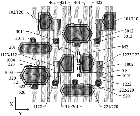
in a second direction perpendicular to the base substrate, the second electrode of the light emitting element of each of the plurality of first color sub-pixels is overlapped with the first data line, the first power signal line and the first connecting portion; for these overlapping parts of the first data line, the first power signal line and the first connecting portion with the second electrode, the overlapping part of the first power signal line and the overlapping part of the first data line are respectively located at both sides of the overlapping part of the first connecting portion, and the first connecting portion comprises a first sub-connecting portion and a first block which are connected with each other, the first block is located at a side of the first sub-connecting portion close to the first power signal line, and both the first sub-connecting portion and the first block are overlapped with the second electrode of the light emitting element;
in the first direction, a size of the first sub-connecting portion is greater than a size of the first block, and a ratio of a minimum distance between edges of the first sub-connecting portion and the first data line which are close to each other to a minimum distance between edges of the first block and the first power signal line which are close to each other is in a range from 0.8 to 1.2.
|