US 12,073,789 B2
Electro-optical device and electronic apparatus
Takashi Toya, Shimosuwa-machi (JP); and Takehiko Kubota, Matsumoto (JP)
Assigned to SEIKO EPSON CORPORATION, Tokyo (JP)
Filed by SEIKO EPSON CORPORATION, Tokyo (JP)
Filed on Jun. 6, 2023, as Appl. No. 18/206,196.
Application 18/206,196 is a continuation of application No. 17/859,318, filed on Jul. 7, 2022, granted, now 11,710,454.
Application 17/859,318 is a continuation of application No. 17/168,421, filed on Feb. 5, 2021, granted, now 11,423,838, issued on Aug. 23, 2022.
Application 17/168,421 is a continuation of application No. 16/734,648, filed on Jan. 6, 2020, granted, now 10,957,254, issued on Mar. 23, 2021.
Application 16/734,648 is a continuation of application No. 15/629,452, filed on Jun. 21, 2017, granted, now 10,553,157, issued on Feb. 4, 2020.
Application 15/629,452 is a continuation of application No. 15/144,186, filed on May 2, 2016, granted, now 9,721,506, issued on Aug. 1, 2017.
Application 15/144,186 is a continuation of application No. 14/678,552, filed on Apr. 3, 2015, granted, now 9,361,830, issued on Jun. 7, 2016.
Application 14/678,552 is a continuation of application No. 13/848,323, filed on Mar. 21, 2013, granted, now 9,030,390, issued on May 12, 2015.
Claims priority of application No. 2012-084743 (JP), filed on Apr. 3, 2012.
Prior Publication US 2023/0317010 A1, Oct. 5, 2023
This patent is subject to a terminal disclaimer.
Int. Cl. G09G 3/32 (2016.01); G09G 3/3208 (2016.01); G09G 3/3241 (2016.01); G09G 3/3291 (2016.01); H01L 27/12 (2006.01); H10K 59/121 (2023.01); H10K 59/123 (2023.01); H10K 59/131 (2023.01); G09G 3/3233 (2016.01)
CPC G09G 3/3241 (2013.01) [G09G 3/3208 (2013.01); G09G 3/3291 (2013.01); H01L 27/124 (2013.01); H01L 27/1255 (2013.01); H10K 59/1213 (2023.02); H10K 59/123 (2023.02); H10K 59/131 (2023.02); G09G 3/3233 (2013.01); G09G 2300/0408 (2013.01); G09G 2300/0439 (2013.01); G09G 2300/0465 (2013.01); G09G 2300/0861 (2013.01); G09G 2310/0289 (2013.01); G09G 2310/0297 (2013.01)] 8 Claims
OG exemplary drawing
 
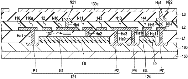
1. An electro-optical device comprising:
a feed line;
a light-emitting element that emits light corresponding to a current supplied via the feed line;
a control line that supplies a signal;
a capacitor that stores a potential;
a first transistor that has a first gate electrode electrically connected to the capacitor, the first transistor controlling the current corresponding to the potential;
a second transistor that has a second gate electrode electrically connected to the control line, the second transistor interrupting the current corresponding to the signal; and
a first insulating layer that has a first contact hole through which the second gate electrode and the control line are electrically connected, wherein
in plan view, the control line overlaps with the second gate electrode, and the first contact hole overlaps with the second gate electrode.