| CPC G09G 3/3233 (2013.01) [H10K 59/1213 (2023.02); H10K 59/1315 (2023.02); G09G 2300/0819 (2013.01); G09G 2310/08 (2013.01)] | 18 Claims |

|
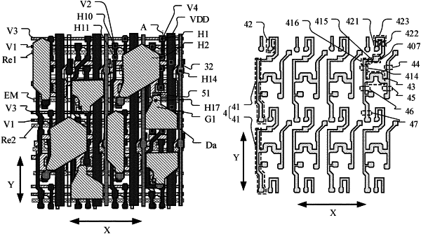
1. A display panel comprising a pixel driving circuit, wherein the display panel further comprises:
a base substrate;
a second conductive layer, disposed on a side of the base substrate and comprising multiple first signal lines, wherein orthographic projections of the multiple first signal lines on the base substrate extend in a first direction and are spaced apart in a second direction, and the first direction and the second direction intersect; and
a third conductive layer, disposed on a side of the second conductive layer away from the base substrate and comprising multiple second signal lines, wherein orthographic projections of the multiple second signal lines on the base substrate extend in the second direction and are spaced apart in the first direction;
wherein the first signal lines and the second signal lines are configured to provide a same first signal to the pixel driving circuit, and at least part of the first signal lines and at least part of the second signal lines are coupled through via holes;
wherein the second conductive layer further comprises multiple third signal lines, wherein orthographic projections of the multiple third signal lines on the base substrate extend in the first direction and are spaced apart in the second direction; and
the third conductive layer further comprises multiple fourth signal lines, wherein orthographic projections of the multiple fourth signal lines on the base substrate extend in the second direction and are spaced apart in the first direction;
wherein the third signal lines and the fourth signal lines are configured to provide a same second signal to the pixel driving circuit, and at least part of the third signal lines and at least part of the fourth signal lines are coupled through via holes.
|
|
18. A display device comprising a display panel, wherein the display panel comprises a pixel driving circuit, and the display panel further comprises:
a base substrate;
a second conductive layer, disposed on a side of the base substrate and comprising multiple first signal lines, wherein orthographic projections of the multiple first signal lines on the base substrate extend in a first direction and are spaced apart in a second direction, and the first direction and the second direction intersect; and
a third conductive layer, disposed on a side of the second conductive layer away from the base substrate and comprising multiple second signal lines, wherein orthographic projections of the multiple second signal lines on the base substrate extend in the second direction and are spaced apart in the first direction;
wherein the first signal lines and the second signal lines are configured to provide a same first signal to the pixel driving circuit, and at least part of the first signal lines and at least part of the second signal lines are coupled through via holes;
wherein the second conductive layer further comprises multiple third signal lines, wherein orthographic projections of the multiple third signal lines on the base substrate extend in the first direction and are spaced apart in the second direction; and
the third conductive layer further comprises multiple fourth signal lines, wherein orthographic projections of the multiple fourth signal lines on the base substrate extend in the second direction and are spaced apart in the first direction;
wherein the third signal lines and the fourth signal lines are configured to provide a same second signal to the pixel driving circuit, and at least part of the third signal lines and at least part of the fourth signal lines are coupled through via holes.
|