| CPC G09G 3/32 (2013.01) [G09G 2300/0842 (2013.01); G09G 2310/0267 (2013.01); G09G 2310/0286 (2013.01); G09G 2310/0289 (2013.01); G09G 2310/0297 (2013.01); G09G 2310/08 (2013.01)] | 20 Claims |

|
1. A device comprising:
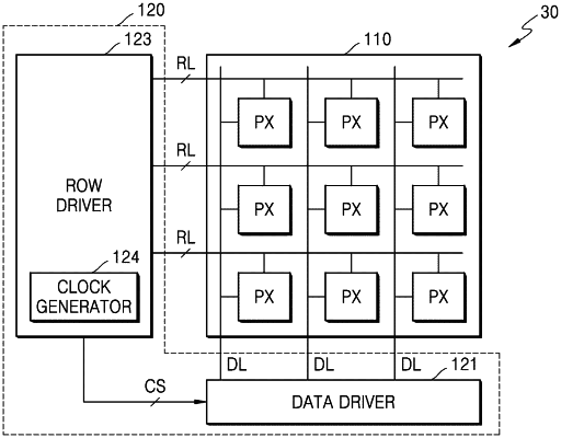
a pixel array including a plurality of rows, and each row of the plurality of rows includes a plurality of pixels;
a row driver configured to,
generate a plurality of control signals,
drive the plurality of rows of the pixel array using the plurality of control signals, and
generate a plurality of clock signals;
a row multiplexer configured to receive the plurality of clock signals, and selectively transmit one clock signal of the plurality of clock signals to the pixel array;
a data driver configured to transmit a plurality of data signals to the pixel array by column units; and
each pixel of the plurality of pixels includes,
a light emitting device,
a shift register configured to receive the selectively transmitted clock signal from the row multiplexer, and generate a width adjusted pulse width modulation (PWM) signal based on a desired brightness level of the light emitting device, and
a transistor configured to transmit a driving current to the light emitting device based on the PWM signal.
|