| CPC G09G 3/32 (2013.01) [G09G 2300/0452 (2013.01); G09G 2310/0275 (2013.01); G09G 2310/0297 (2013.01)] | 18 Claims |

|
1. An array substrate, comprising:
a plurality of first selection circuits, wherein each first selection circuit comprises at least two first selection transistors and at least two first anticreeping transistors, and each first selection transistor is correspondingly connected with one first anticreeping transistor of the at least two first anticreeping transistors in series; and
for each first selection transistor and the one first anticreeping transistor correspondingly connected in series in each first selection circuit:
when a first selection transistor is turned on under control of a first turn-on signal provided by a first control signal terminal, a corresponding first anticreeping transistor is turned on under control of a second turn-on signal provided by a second control signal terminal to form a conducting path between a data signal terminal and a corresponding first selection transistor; and
when a first selection transistor is turned off under control of a first turn-off signal provided by the first control signal terminal, a corresponding first anticreeping transistor is turned off under control of a second turn-off signal provided by the second control signal terminal to make a corresponding first selection transistor and the data signal terminal disconnected, wherein a voltage of the first turn-off signal is greater than a voltage of the second turn-off signal;
wherein the array substrate further comprises a plurality of sub pixels arranged in an array, wherein
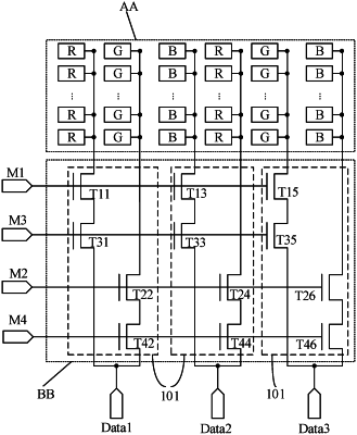
the first control signal terminal comprises a first sub signal terminal and a second sub signal terminal, and the second control signal terminal comprises a third sub signal terminal and a fourth sub signal terminal; wherein the first sub signal terminal, the second sub signal terminal, the third sub signal terminal and the fourth sub signal terminal are different signal terminals for independently providing different timing signals each oscillating between a high and low state;
the data signal terminal comprises a plurality of sub data signal terminals, and each sub data signal terminal is correspondingly coupled with one first selection circuit of the plurality of first selection circuits;
each first selection circuit comprises: a first transistor, a second transistor, a third transistor and a fourth transistor, wherein
the first transistor and the second transistor are first selection transistors, and the third transistor and the fourth transistor are first anticreeping transistors;
a gate electrode of the first transistor is coupled with the first sub signal terminal, a first electrode of the first transistor is coupled with a second electrode of the third transistor, and a second electrode of the first transistor is coupled with an odd-number column of sub pixels;
a gate electrode of the third transistor is coupled with the third sub signal terminal, and a first electrode of the third transistor is coupled with a corresponding sub data signal terminal;
a gate electrode of the second transistor is coupled with the second sub signal terminal, a first electrode of the second transistor is coupled with a second electrode of the fourth transistor, and a second electrode of the second transistor is coupled with an even-number column of sub pixels; and
a gate electrode of the fourth transistor is coupled with the fourth sub signal terminal, and a first electrode of the fourth transistor is coupled with the corresponding sub data signal terminal.
|