| CPC G09G 3/2092 (2013.01) [G09G 2310/0286 (2013.01)] | 19 Claims |
|
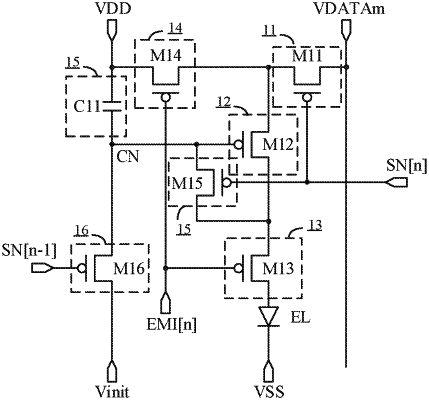
1. A shift register unit, comprising a first input circuit, a second input circuit, an output circuit, a first control circuit, and a second control circuit,
wherein the first input circuit is electrically connected to a first node, and is configured to transmit an input signal to the first node under control of a first clock signal;
the second input circuit is electrically connected to the first node and a second node, and is configured to control a level of the second node under control of a level of the first node or the first clock signal;
the first control circuit is electrically connected to the second node and a third node, and is configured to control a level of the third node under control of the level of the second node and a second clock signal;
the output circuit is electrically connected to the third node, a second voltage signal line and an output terminal, and is configured to output an output signal to the output terminal under control of the level of the third node; and
the second control circuit is electrically connected to the first node, the third node and a first voltage signal line, and is configured to control the level of the third node under control of the level of the first node, and
wherein the first voltage signal line and the second voltage signal line are two different voltage signal lines, and wherein a pulse width of the input signal is different from a pulse width of the first clock signal, and the pulse width of the input signal is different from a pulse width of the second clock signal.
|