| CPC G09G 3/2092 (2013.01) [G09G 2300/0408 (2013.01); G09G 2300/0426 (2013.01); G09G 2310/0267 (2013.01); G09G 2310/0286 (2013.01); G11C 19/28 (2013.01)] | 18 Claims |
|
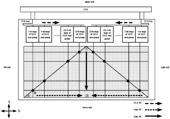
1. A display panel, comprising:
Q rows of first scanning line groups arranged sequentially along a column direction;
M columns of second scanning line groups arranged sequentially along a row direction; and
at least one gate drive circuit, located on a side of a Q-th row of the first scanning line groups away from a (Q−1)-th row of the first scanning line groups, wherein:
each gate drive circuit comprises Q columns of shift register unit groups cascaded in stages;
a q-th stage of the shift register unit groups is connected with a q-th row of the first scanning line groups through at least one column of the second scanning line groups;
M≥Q>1;
q=1 or 1<q≤Q; and
M, Q, and q are all positive integers, wherein
in the gate drive circuit, the shift register unit groups from a 1-st stage to a Q-th stage are arranged sequentially along the row direction;
the gate drive circuit comprises a first gate drive circuit and a second gate drive circuit; and
the Q-th stage of the shift register unit groups in the first gate drive circuit is disposed adjacent to the Q-th stage of the shift register unit groups in the second gate drive circuit or adjacent to the 1-st stage of the shift register unit groups in the second gate drive circuit.
|