| CPC G06V 40/1318 (2022.01) [G06F 3/042 (2013.01); G06F 1/163 (2013.01)] | 7 Claims |

|
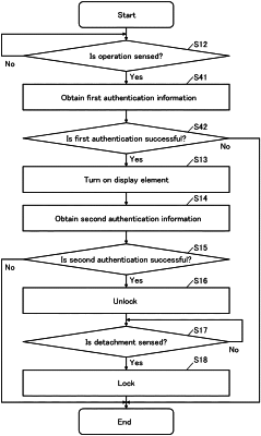
1. An electronic device comprising:
a pixel portion;
a sensor portion;
an authentication portion; and
a housing,
wherein the pixel portion comprises a display element and a light-receiving element,
wherein the sensor portion is configured to obtain first authentication information,
wherein the first authentication information is one of a blood glucose level, a cholesterol concentration in blood, and a neutral fat concentration in the blood,
wherein the authentication portion is configured to perform first authentication processing using the first authentication information,
wherein the pixel portion is configured to turn on the display element after the authentication portion has determined that the first authentication information matches data of a user registered in advance and retained in a memory portion of the electronic device,
wherein, after the display element is turned on, the pixel portion is configured to obtain second authentication information by capturing an image of a target object touching the pixel portion using the light-receiving element,
wherein the authentication portion is configured to perform second authentication processing using the second authentication information,
wherein the housing comprises a first surface and a second surface opposite to the first surface,
wherein the pixel portion is positioned on the first surface, and
wherein the sensor portion is positioned on the second surface.
|