| CPC G06T 7/001 (2013.01) [G01N 21/9501 (2013.01); H01L 21/67196 (2013.01); H01L 21/67288 (2013.01); G01N 2201/0634 (2013.01); G06T 2207/30148 (2013.01)] | 17 Claims |

|
1. A defect inspection system comprising:
an information-obtainer arranged over a transferring member to successively photograph a surface of at least one substrate moving between at least two apparatuses; and
a defect inspector generating an image signal based on information of the substrate provided from the information-obtainer and comparing the image signal with a reference to detect a defect of the substrate,
wherein the information-obtainer comprises:
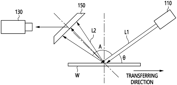
a light source configured to provide the substrate with an incident light; and
an optical detector collecting a reflected light from the substrate to generate an electrical signal with respect to the reflected light, wherein the optical detector is configured to move along a transferring direction of the substrate, and
wherein the light source comprises a first sub-light source configured to irradiate a first light to a first substrate, which transfers first, and a second sub-light source configured to irradiate a second light to a second substrate, which transfers later.
|