| CPC G06F 30/392 (2020.01) [H01L 27/0886 (2013.01); H01L 29/7831 (2013.01)] | 20 Claims |

|
1. A method, comprising:
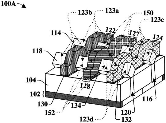
removing portions of a substrate to form a continuous fin protruding from an upper surface of the substrate, wherein the continuous fin has a first dopant concentration;
performing a doping process to selectively increase a dopant concentration of a first portion of the continuous fin such that the first portion of the continuous fin has a second dopant concentration that is greater than the first dopant concentration;
forming a first gate electrode over a second portion of the continuous fin;
forming a second gate electrode over a third portion of the continuous fin, wherein the first portion of the continuous fin is between the second portion and the third portion of the continuous fin;
forming a dummy gate electrode over the first portion of the continuous fin;
removing upper portions of the continuous fin that are arranged between the first gate electrode, the second gate electrode, and the dummy gate electrode; and
forming source/drain regions between the first gate electrode, the second gate electrode, and the dummy gate electrode.
|