| CPC G06F 30/392 (2020.01) [G06F 30/323 (2020.01); G06F 30/398 (2020.01); G06F 2111/20 (2020.01)] | 20 Claims |

|
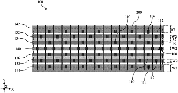
1. An analog standard cell fabricated on a substrate, comprising:
a first active region and a second active region extending side-by-side along a first direction; and
a plurality of conductive lines in a first metal layer over the first active region and the second active region, the plurality of conductive lines comprising:
a first conductive line and a second conductive line extending along the first direction and disposed directly over the first active region,
a third conductive line and a fourth conductive line extending along the first direction and disposed directly over the second active region,
a middle conductive line disposed between the second conductive line and the third conductive line,
a first power line spaced apart from the middle conductive line by the first conductive line and the second conductive line, and
a second power line spaced apart from the middle conductive line by the third conductive line and the fourth conductive line.
|