| CPC G06F 30/392 (2020.01) [G06F 30/398 (2020.01); H05K 3/0005 (2013.01); H05K 3/1225 (2013.01)] | 9 Claims |

|
1. A stencil step design method, comprising:
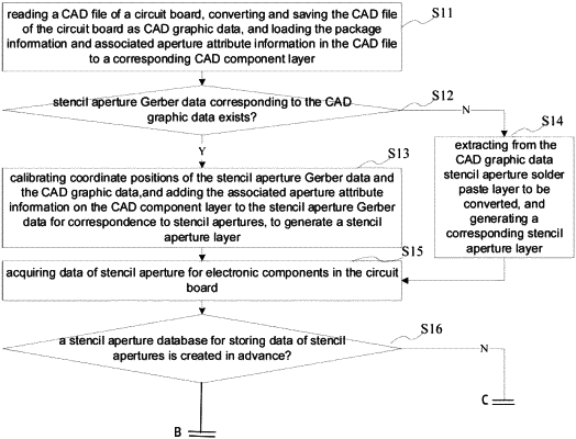
acquiring data of stencil apertures for electronic components in a circuit board, and identifying the stencil apertures for electronic components one by one to determine whether the stencil apertures need to be stepped; and
if yes, performing step design for the stencil apertures that need to be stepped according to preset step rules corresponding to the stencil apertures for electronic components one by one so as to generate a stencil step design file with the step design, and outputting the stencil step design file; and if not, ending the stepped stencil design and outputting an aperture design file;
wherein after acquiring data of stencil apertures for electronic components in a circuit board, the stencil step design method further comprises:
searching whether a stencil aperture database for storing data of stencil apertures is created in advance; if yes, automatically matching a step thickness attribute of the stencil apertures for electronic components in the stencil aperture database; and if not, adding the step thickness attribute to the stencil apertures that need to be stepped in the stencil aperture data.
|