US 12,073,162 B2
Capacitive isolation structure insert for reversed signals
Cheok-Kei Lei, Hsinchu (TW); Jerry Chang Jui Kao, Hsinchu (TW); Chi-Lin Liu, Hsinchu (TW); Hui-Zhong Zhuang, Hsinchu (TW); Zhe-Wei Jiang, Hsinchu (TW); and Chien-Hsing Li, Hsinchu (TW)
Assigned to TAIWAN SEMICONDUCTOR MANUFACTURING COMPANY, LTD., Hsinchu (TW)
Filed by TAIWAN SEMICONDUCTOR MANUFACTURING COMPANY, LTD., Hsinchu (TW)
Filed on Nov. 30, 2022, as Appl. No. 18/060,118.
Application 18/060,118 is a continuation of application No. 17/195,133, filed on Mar. 8, 2021, granted, now 11,526,649.
Application 17/195,133 is a continuation of application No. 16/514,210, filed on Jul. 17, 2019, granted, now 10,943,050, issued on Mar. 9, 2021.
Claims priority of provisional application 62/753,363, filed on Oct. 31, 2018.
Prior Publication US 2023/0090213 A1, Mar. 23, 2023
This patent is subject to a terminal disclaimer.
Int. Cl. G06F 30/367 (2020.01); G06F 30/20 (2020.01); G06F 30/392 (2020.01); G06F 30/394 (2020.01); G06F 30/398 (2020.01); H01L 23/522 (2006.01); H01L 27/02 (2006.01)
CPC G06F 30/367 (2020.01) [G06F 30/20 (2020.01); G06F 30/392 (2020.01); G06F 30/394 (2020.01); G06F 30/398 (2020.01); H01L 23/5223 (2013.01); H01L 27/0207 (2013.01)] 20 Claims
OG exemplary drawing
 
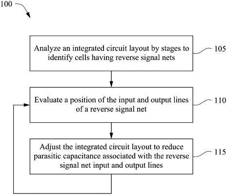
1. A method of modifying an integrated circuit layout, comprising:
determining whether a first conductive line and a second conductive line are subject to a parasitic capacitance above a parasitic capacitance threshold;
adjusting the integrated circuit layout by moving the first conductive line in the integrated circuit layout in response to determining to move the first conductive line; and
inserting an isolation structure between the first and second conductive lines in the integrated circuit layout in response to determining not to move the first conductive line, wherein inserting the isolation structure comprises inserting the isolation structure along a routing track of the integrated circuit layout.