| CPC G06F 3/0446 (2019.05) [G06F 3/0412 (2013.01); G06F 3/0448 (2019.05); G06F 2203/04111 (2013.01); G06F 2203/04112 (2013.01)] | 20 Claims |
|
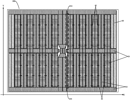
1. A display panel, comprising:
a display substrate; and
a touch electrode layer, which is arranged on a light outgoing side of the display substrate, and comprises at least one first electrode and at least one second electrode, which intersect with each other and are insulated from each other;
wherein the display panel further comprises:
an additional electrode layer, which is arranged in a layer different from the touch electrode layer and comprises at least one first additional electrode; wherein an orthographic projection of the at least one first additional electrode on the display substrate at least partially overlaps an orthographic projection of the at least one first electrode on the display substrate; and
an insulating layer, which is arranged between the additional electrode layer and the touch electrode layer; wherein the at least one first additional electrode is connected to the at least one first electrode through at least one first via in the insulating layer;
the additional electrode layer further comprises at least one second additional electrode, which is insulated from the at least one first additional electrode; and
an orthographic projection of the at least one second additional electrode on the display substrate at least partially overlaps the orthographic projection of the at least one second electrode on the display substrate, and the at least one second additional electrode is connected to the at least one second electrode through at least one second via in the insulating layer; and
the orthographic projection of an edge of each first electrode of the at least one first electrode, close to an adjacent second electrode of this first electrode, on the display substrate comprises a first edge region, and the orthographic projection of a first addition electrode of the at least one first additional electrode, corresponding to this first electrode, on the display substrate overlaps the first edge region; and
the orthographic projection of an edge of each second electrode of the at least one second electrode, close to an adjacent first electrode of this second electrode, on the display substrate comprises a second edge region, and the orthographic projection of a second additional electrode of the at least one second additional electrode, corresponding to this second electrode, on the display substrate overlaps the second edge region; and
the additional electrode layer further comprises at least one bridge portion; and
the at least one bridge portion is connected to the at least one first additional electrode; the at least one first electrode comprises two first electrode blocks at both sides of one of the at least one second electrode; the at least one bridge portion electrically connects the two first electrode blocks together through at least two third vias in the insulating layer;
or
the at least one bridge portion is connected to the at least one second additional electrode; the at least one second electrode comprises two second electrode blocks at both sides of one of the at least one first electrode; the at least one bridge portion electrically connects the two second electrode blocks together through at least two third vias in the insulating layer.
|