| CPC G06F 3/0412 (2013.01) [G06F 2203/04102 (2013.01)] | 18 Claims |

|
1. A display panel, comprising:
a base substrate; and
a pixel driving circuit layer, an anode layer, a light emitting layer, a cathode layer, an encapsulation layer and a touch function layer sequentially disposed on the base substrate,
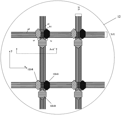
wherein the display panel comprises a plurality of light transmitting regions and a plurality of pixel cell regions, a plurality of traces of the pixel driving circuit layer are connected between adjacent pixel cell regions, and there are slits between adjacent traces,
wherein an orthographic projection of a wiring of the touch function layer on the base substrate overlaps with an orthographic projection of the slits on the base substrate;
wherein the display panel comprises a first display region and a second display region different from the first display region, the second display region comprises the plurality of light transmitting regions and the plurality of pixel cell regions; and
wherein the number of pixel cells per unit area in the first display region is greater than the number of pixel cells per unit area in the second display region.
|