| CPC G06F 13/20 (2013.01) [G06N 10/40 (2022.01); H01L 29/423 (2013.01); H01L 29/42316 (2013.01); H01L 29/66977 (2013.01); H03K 17/92 (2013.01); H10N 60/11 (2023.02); H10N 60/128 (2023.02); H10N 69/00 (2023.02); G06F 2213/40 (2013.01)] | 13 Claims |

|
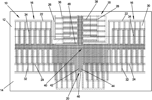
1. An electronic component (10), which is formed by a semiconductor component or a semiconductor-like structure having gate electrode assemblies (16, 18, 20) for moving a quantum dot (52), comprising:
a substrate (12) with a two-dimensional electron gas or electron hole gas;
electrical contacts for connecting the gate electrode assemblies (16, 18, 20) to voltage sources;
a first gate electrode assembly (16) having first gate electrodes (22, 24),
the first gate electrode assembly (16) being arranged on a surface (14) of the electronic component, for producing a potential well (50) in the substrate (12),
the first gate electrode assembly (16) having parallel first electrode fingers (32, 34),
wherein the first electrode fingers (32, 34) are interconnected in a periodically alternating manner, which causes an almost continuous movement of the potential well (50) through the substrate (12), whereby the quantum dot (52) is transported in one direction together with this potential well (50);
a second gate electrode assembly (18) having second gate electrodes (26, 28), the second gate electrode assembly (18) being provided with a different direction at a branch (40) to the first gate electrode assembly (16);
the second gate electrode assembly (18) having parallel second electrode fingers (36, 38),
wherein the second electrode fingers (36, 38) are interconnected in a periodically alternating manner, which causes an almost continuous further movement of the potential well (50) through the substrate (12), whereby the quantum dot (52) in the potential well (50) can be moved in a different direction of travel.
|