US 12,072,817 B2
Flash memory device having a calibration mode
Pravin Kumar Venkatesan, Fremont, CA (US); Liji Gopalakrishnan, Sunnyvale, CA (US); Kashinath Ullhas Prabhu, Bangalore (IN); and Makarand Ajit Shirasgaonkar, Bangalore (IN)
Assigned to Rambus Inc., San Jose, CA (US)
Filed by Rambus Inc., San Jose, CA (US)
Filed on Jun. 29, 2023, as Appl. No. 18/216,439.
Application 18/216,439 is a continuation of application No. 18/082,446, filed on Dec. 15, 2022, granted, now 11,829,308.
Application 18/082,446 is a continuation of application No. 17/849,450, filed on Jun. 24, 2022, granted, now 11,803,489.
Application 17/849,450 is a continuation of application No. 16/709,506, filed on Dec. 10, 2019, granted, now 11,372,784, issued on Jun. 28, 2022.
Application 16/709,506 is a continuation of application No. 16/145,837, filed on Sep. 28, 2018, granted, now 10,509,741, issued on Dec. 17, 2019.
Application 16/145,837 is a continuation of application No. 15/616,785, filed on Jun. 7, 2017, granted, now 10,089,256, issued on Oct. 2, 2018.
Application 15/616,785 is a continuation of application No. 14/080,724, filed on Nov. 14, 2013, granted, now 9,715,467, issued on Jul. 25, 2017.
Claims priority of provisional application 61/730,018, filed on Nov. 26, 2012.
Prior Publication US 2023/0418770 A1, Dec. 28, 2023
This patent is subject to a terminal disclaimer.
Int. Cl. G06F 13/16 (2006.01)
CPC G06F 13/1668 (2013.01) [Y02D 10/00 (2018.01)] 20 Claims
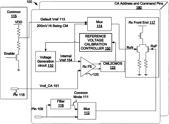
OG exemplary drawing
 
1. A method of operation in a flash integrated circuit (IC) memory device having an array of memory cells, the method comprising:
initializing an interface to receive control, address and data signals, wherein, at boot-up, the interface is operable to receive, using an internal reference voltage, signals having a first voltage swing at a first signaling frequency;
receiving a clock signal;
receiving a first command using the clock signal, wherein the first command specifies calibration of the interface during a calibration mode, wherein the calibration mode is used to calibrate the interface to operate at a second signaling frequency and receive signals having a second voltage swing, wherein the second voltage swing is smaller than the first voltage swing and the second signaling frequency is higher than the first signaling frequency; and
the interface, during the calibration mode, receiving a calibration pattern at the second signaling frequency.