| CPC G06F 1/3296 (2013.01) [H04B 5/77 (2024.01)] | 20 Claims |

|
1. An electronic device, comprising:
a control unit;
a power supply circuit configured to generate a first supply voltage;
an antenna configured to:
receive a radio frequency signal when the control unit is in an OFF state, and
transmit a first voltage to the control unit to power the control unit by a second supply voltage for a duration of a booting sequence of the control unit, the first voltage being a representative of the radio frequency signal; and
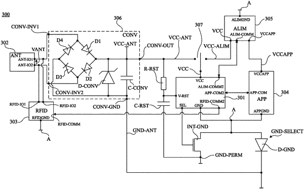
a conversion circuit coupled to the antenna and the control unit, the conversion circuit comprising:
a voltage rectifying diode bridge configured to convert the first voltage from AC to DC, the voltage rectifying diode bridge having a first output terminal and a second output terminal, wherein the second supply voltage equals a potential difference between the first output terminal and the second output terminal, a potential at the second output terminal being at a first reference potential,
a first diode having an anode terminal coupled to the first output terminal, a cathode terminal of the first diode coupled to the second output terminal, and
a capacitor having a first terminal coupled to the first output terminal, a second terminal of the capacitor coupled to the second output terminal.
|